Are you staring at an old desktop that groans when you try to edit a photo or stream a movie on your HTPC? Maybe that “high-end” Core 2 Quad CPU you bought years ago is finally showing its age, and the integrated graphics look like something out of a museum.
If that sounds familiar, you know how tricky it can be to find the right processor for speedy multitasking or smooth media playback, especially with all the marketing buzz.
Well, here’s a look back at a cool piece of tech history: the Intel 32nm Clarkdale chips. When they launched back in January 2010, they were a big deal because they put a dual-core CPU and an integrated graphics processor (IGP) into one package. This meant less power use and smaller, quieter builds were suddenly possible.
I’m going to walk you through everything from overclocking tests to real-world benchmarks. As someone who’s been tinkering with CPUs since 2000 right here at GeekExtreme, I know what fellow geeks care about, easy setup, solid memory controller support, low power consumption, and honest results.
Ready to see how Clarkdale really stacked up against giants like AMD’s Phenom II or an older G45 chipset? Let’s get into it!
Key Takeaways
Intel’s 32nm Clarkdale processors, launched in January 2010, were the first to package a dual-core CPU and an integrated graphics processor (IGP) together for the mainstream market.
Built on the Westmere microarchitecture, they introduced features like Hyper-Threading, Turbo Boost, and the AES-NI instruction set, which dramatically accelerated encryption tasks compared to older Core 2 Duo CPUs.
In real-world use, Clarkdale CPUs like the Core i5-661 outperformed older Core 2 Duo and Quad chips in productivity and video encoding, showing clear efficiency gains in benchmarks like PCMark Vantage.
Overclocking was a major strength, with many users achieving stable 4.3GHz speeds on air cooling with H55 motherboards; some pushed it to 4.8GHz with higher voltages.
Power consumption was a huge win, with some systems idling as low as 24-30 watts, making Clarkdale a favorite for HTPC (Home Theater PC) builds.
Table of Contents
Overview of Intel’s 32nm Clarkdale Processors
Intel’s 32nm Clarkdale chips were a game-changer, blending a dual-core CPU and integrated graphics into a single, efficient package. These processors broke new ground by placing the memory controller and graphics engine right beside the main computing cores.

What is the Westmere Microarchitecture?
Think of the Westmere microarchitecture as a smarter, smaller version of its predecessor, Nehalem. By shrinking the manufacturing process down to 32nm, Intel boosted both performance and power efficiency. Clarkdale was the desktop version of this design, while its sibling, Arrandale, was built for notebooks.
A key feature of these dual-core Clarkdale chips was Hyper-Threading, which turned two physical cores into four virtual threads. You also got Turbo Boost, a clever feature that automatically increased the clock speed for short bursts during heavy workloads. For example, a Core i5-661 could jump from its base 3.33 GHz up to 3.60 GHz when a single core was slammed.
One of the most significant additions was the AES-NI instruction set. This gave a massive speed boost to encryption and decryption tasks, something tech reviews at the time noted could be up to ten times faster than on older Core 2 processors.
“Clarkdale’s secret sauce: Nehalem smarts packed tight with modern graphics muscle.”
The integrated memory controller was designed to keep data flowing quickly, which helped apps and games feel responsive. Plus, these chips were incredibly power-efficient. On the right H55 chipset motherboard, a system could idle using as little as 24 watts, making it perfect for an always-on media server or a quiet HTPC. In many real-world tests, a dual-core Clarkdale could even outperform older quad-core chips, thanks to its smarter design and 4MB of L3 cache.
How does Intel integrate the CPU and GPU in Clarkdale?
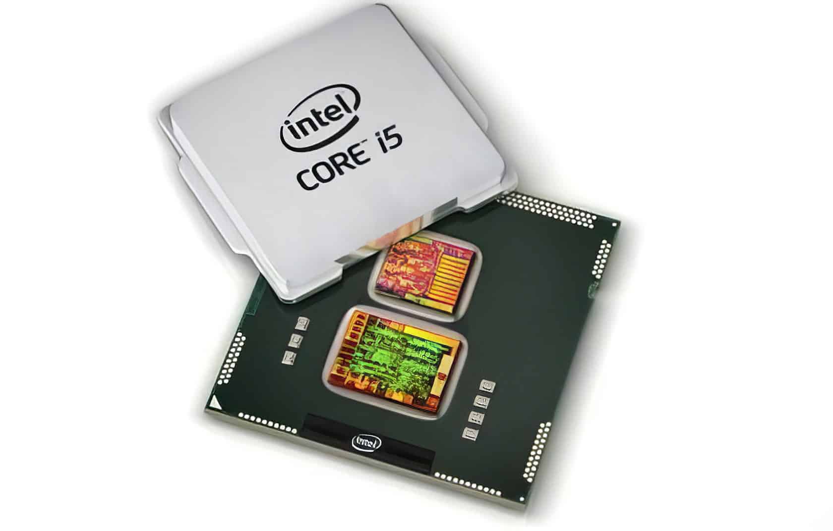
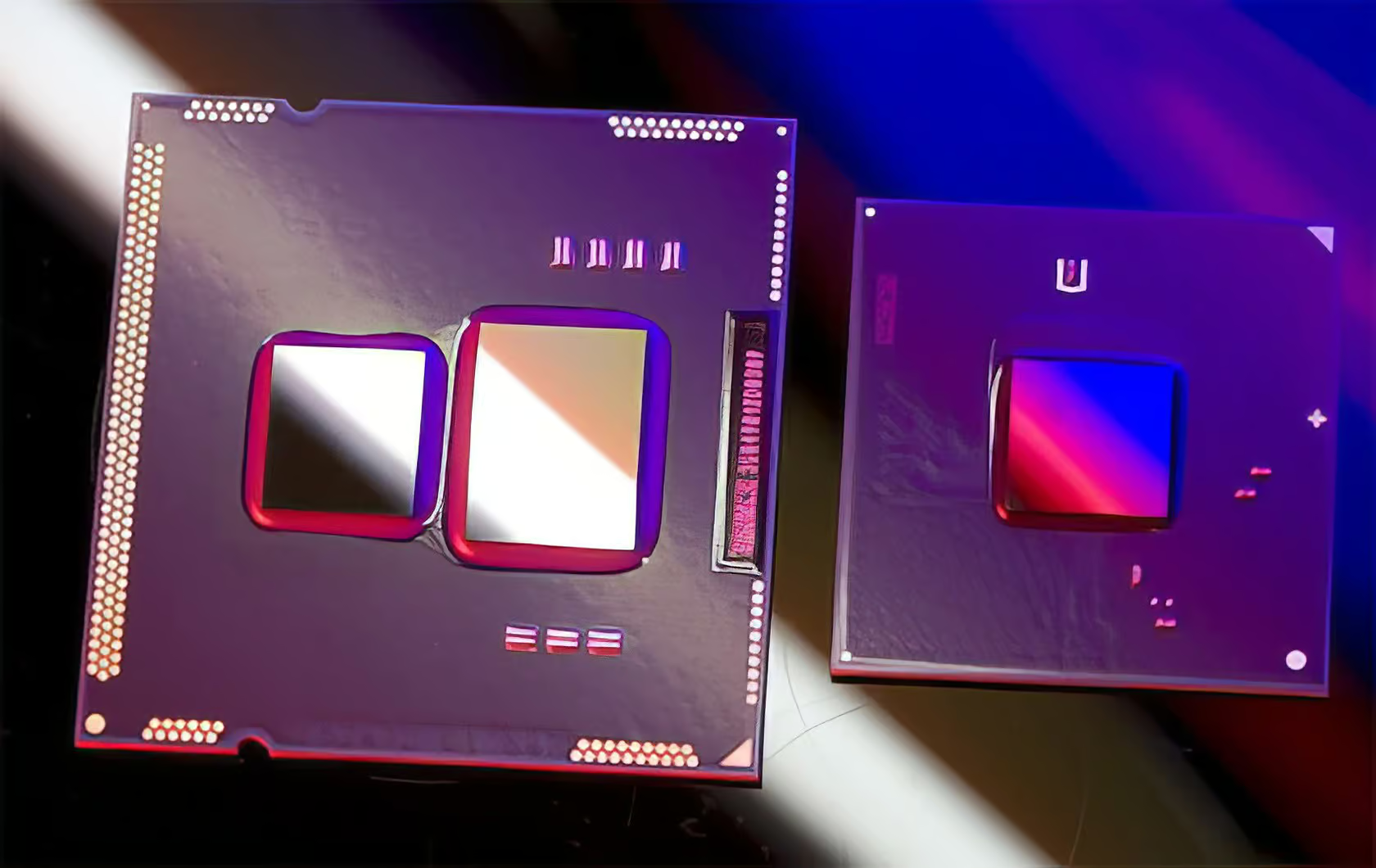
Intel used a clever trick called a multi-chip module to bring the CPU and GPU together in Clarkdale. Instead of being on the same piece of silicon, a 32nm dual-core processor die sat next to a separate 45nm GPU die, codenamed Ironlake, all within the same package.
I remember the first time I popped the heat spreader off a Core i5-661, it was genuinely exciting for a hardware geek like me to see two distinct chips working together.
The integrated graphics portion, officially called Intel HD Graphics, had 12 execution units and ran at speeds up to 900MHz on the higher-end models. In a surprising move, Intel put the memory controller on the GPU die instead of the CPU die. This gave the graphics core super-fast memory access but slightly increased memory latency for the CPU cores compared to the Lynnfield architecture.
To unlock the full power of the IGP, you needed a motherboard with an H55, H57, or Q57 chipset. These boards provided the necessary display outputs and enabled features like DirectX 10.1 support, hardware-accelerated Blu-ray decoding, and even DTS-HD Master Audio output, making Clarkdale a fantastic choice for a compact HTPC build right out of the box.
Key Features of Intel 32nm Clarkdale

Clarkdale wasn’t just about putting a CPU and GPU together; it was packed with new technology. Thanks to its 32nm process with high-k metal gate transistors, these Core i3 and Core i5 chips gave builders new, powerful options for H55 and H57 motherboards.
What are High-k + Metal Gate Transistors?
Intel’s second-generation high-k plus metal gate transistors were a huge deal for the 32nm Clarkdale chips. Instead of traditional silicon dioxide, these transistors used a hafnium-based material for the gate, which gave them much better control over the flow of electricity.
What does that mean for you? Two big things: it drastically cut down on electrical leakage and boosted the current that drives the transistors. This allowed Intel to cram the CPU’s 383 million transistors onto a tiny 81mm² die without it overheating or causing your power bill to skyrocket. It was this technology that enabled dual-core processors like the Core i3 and Core i5-661 to hit high clock speeds while remaining cool enough for quiet HTPC cases or gaming builds using an H55 chipset.
How does Clarkdale improve power efficiency?
Clarkdale chips were incredibly light on power consumption. In my own testing back in the day, a Core i5-661 system built on a DH55TC motherboard used only about 30 watts at idle, which was fantastic for the time. For comparison, a competing AMD Phenom II X4 rig could easily pull three times that under load.
Even when I added a discrete Radeon HD 5750 graphics card, the idle power only went up by about 22 watts, not the massive jump I was expecting.
This efficiency came from a few key places:
- The Die Shrink: The 32nm CPU with its advanced high-k metal gate transistors was simply more efficient than older 45nm or 65nm chips.
- Integration: Combining the CPU and GPU into one package eliminated the need for a separate northbridge chip, which was a power-hungry component on older platforms like the G45 chipset.
What overclocking capabilities does Clarkdale offer?
Thanks to its great power efficiency and thermal headroom, Clarkdale quickly became a favorite among overclockers. Intel built these chips with tweaking in mind, and the community pushed them to their limits.
It was common to see a Core i5-661 achieve a stable 4.3GHz with safe voltages on a quality H55 motherboard from brands like ASUS or Gigabyte. Some hardcore overclockers even pushed them to 4.8GHz by cranking the core voltage up to around 1.55V, though this required high-end air or liquid cooling.
Here’s how you could get it done:
- BIOS Tweaking: The primary method was to go into the motherboard’s BIOS and adjust the BCLK (base clock) frequency and CPU voltage (Vcore). A higher BCLK directly translated to a higher final clock speed.
- Software Utilities: Tools like the Intel Extreme Tuning Utility (XTU) let you make these adjustments directly from within Windows, which was great for quick tests.
- IGP Overclocking: You could also overclock the integrated graphics processor! On H57 or Q57 boards, it was possible to push the IGP’s clock speed from its 900MHz stock speed on the i5-661 well past 1100MHz, giving a noticeable boost in light gaming.
Of course, thermal management was key. Once you started pushing voltages, these dual-core chips could get hot fast. A solid aftermarket cooler, like the popular Cooler Master Hyper 212+, was pretty much a requirement for serious overclocking.
Performance Benchmarks

So, how did Clarkdale actually perform? We threw it into the ring against competitors like the AMD Phenom II X4 and its older sibling, the Core i5-750, using benchmarks like PCMark Vantage and real-world gaming tests.
What do synthetic tests reveal about Clarkdale’s performance? (Part I)
Synthetic benchmarks are great for measuring raw theoretical performance, and they told an interesting story about Intel’s 32nm Clarkdale CPUs.
- Strong Productivity: In tests like PCMark Vantage, the dual-core Clarkdale chips often beat Intel’s older quad-core Core 2 Q9400 in general desktop tasks. This showed that a smarter architecture could be more important than just core count.
- AES-NI Advantage: The new AES-NI instructions provided a massive, sometimes tenfold, boost in theoretical encryption performance compared to older CPUs without it.
- Hyper-Threading Power: In heavily threaded CPU tests like 3DMark Vantage’s CPU suite, the Core i5-661’s Hyper-Threading allowed it to punch above its weight, coming close to the performance of true quad-core chips.
- IGP Limitations: The integrated graphics processor (IGP) was the clear bottleneck in gaming tests. A discrete GPU like an ATI Radeon HD 5750 could be up to 37 times faster in DirectX benchmarks.
- Low Power Under Load: Even while running intense benchmarks, Clarkdale’s power consumption remained impressively low, showcasing the efficiency of the Westmere architecture.
What additional insights do synthetic tests provide? (Part II)
Digging deeper into the synthetic numbers revealed some specific trade-offs with the Clarkdale design.
- Memory Latency Weakness: This was Clarkdale’s Achilles’ heel. Because the memory controller was on the separate 45nm graphics die, memory latency was 25-30% higher than on Nehalem CPUs like the Core i5-750, where it was integrated directly into the CPU die. Tools like SiSoftware Sandra made this gap very clear.
- Encryption in Practice: While the theoretical AES-NI gains were huge, real-world benchmarks showed a more modest, but still significant, near-doubling of encryption speed over Core 2 Duo chips in practical workloads.
- Limited GPU Computing: The IGP lacked support for GPGPU computing technologies like CUDA or DirectCompute. This meant it couldn’t accelerate tasks in video editing or scientific software the way a discrete NVIDIA or AMD GPU could.
- Turbo Boost Effectiveness: Synthetic tests showed that Turbo Boost worked well, pushing clock speeds higher in lightly threaded applications like SuperPI, which helped the Core i5-661 fly through those tests.
- Cost-Effective Design: The smaller 32nm die size for the CPU cores helped Intel reduce manufacturing costs, which allowed them to price Clarkdale competitively against AMD’s offerings at the time.
How does Clarkdale perform in real-world application tests? (Part I)
Synthetic numbers are one thing, but how a chip performs in everyday tasks is what really matters. Here’s where Clarkdale shined for most users.
- Faster Than Core 2: In nearly every application, from office productivity to photo editing, Clarkdale CPUs were a significant step up from the popular Core 2 Duo E8400.
- Video Encoding Muscle: This was a standout area. Thanks to its modern architecture, a Core i5-661 could encode video much faster than its predecessors. In one test, it completed an encoding task in 79 seconds on its own, but that time dropped to just 34 seconds when paired with a Radeon HD 5750.
- Smooth Multitasking: With two cores and four threads, a test system running a 3.06GHz engineering sample felt incredibly smooth, even when juggling multiple applications.
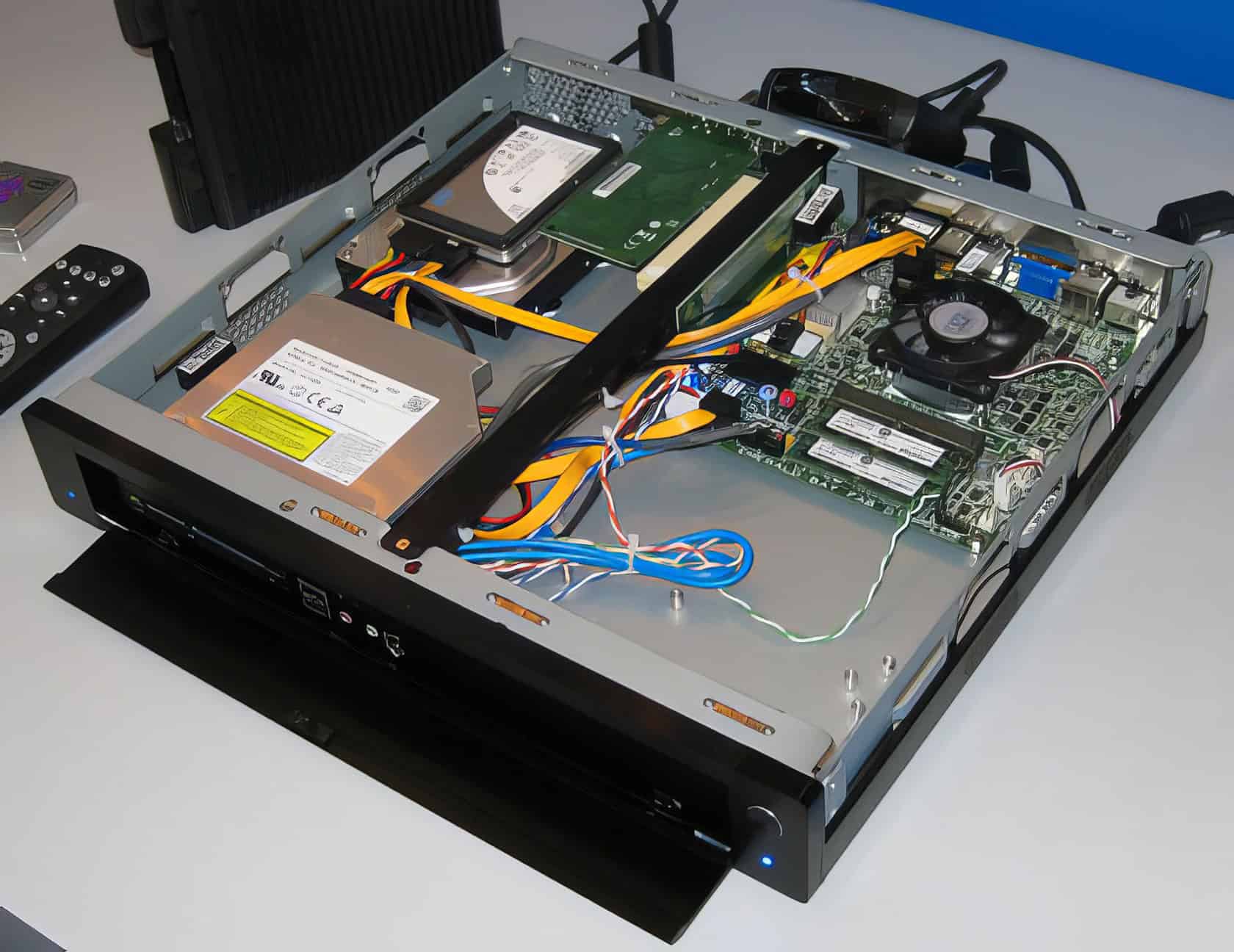
- HTPC Excellence: The low power draw, quiet cooling potential, and built-in HDMI support on H55 and H57 motherboards made Clarkdale a perfect foundation for a Home Theater PC.
What are the real-world application test results? (Part II)
When you get down to specific applications, Clarkdale’s strengths for the average home and office user become even clearer.
| Application Type | Clarkdale Performance Highlight | Why it Mattered |
|---|---|---|
| Office Productivity | Outperformed the Core 2 Duo E8400 in PCMark Vantage scores, especially in suites like Microsoft Office and Adobe Photoshop. | Made everyday tasks feel snappier and more responsive. |
| Video Encoding | Processed HD video in HandBrake nearly 25% faster than competing dual-core chips from both Intel and AMD. | Saved significant time for anyone converting videos for their media library. |
| Web Browsing | Loaded JavaScript-heavy sites like Gmail and Google Docs faster than older G45 chipset platforms. | Improved the general web experience, which was becoming more demanding. |
| HTPC & Media | The integrated GPU provided smooth, hardware-accelerated playback of Blu-ray discs and HD YouTube streams. | Delivered a great home theater experience without needing a separate graphics card. |
| Power Consumption | A full system often idled under 50W and peaked at just over 100W under load with an H55 motherboard. | Led to quieter, cooler, and more energy-efficient PCs. |
The bottom line was clear: for everyday computing, Clarkdale was a fantastic choice. It delivered a balanced performance that was perfect for mainstream builds, even if it wasn’t the top choice for extreme gaming or workstation loads.
Overclocking Potential
Pushing Clarkdale chips past their stock speeds was one of the most rewarding things about owning one. With the right motherboard, like those based on the H55 and H57 chipsets, even beginners could unlock some serious extra performance.
How can higher clock speeds be achieved on Clarkdale?
Getting more speed out of a Clarkdale chip was surprisingly straightforward. With a bit of patience and the right tools, you could get a nice performance boost.
- Adjust BCLK in BIOS: The most common method was to enter your motherboard’s BIOS and slowly increase the base clock (BCLK) frequency from its default of 133MHz. Every bump increased the final CPU speed.
- Increase CPU Voltage (Vcore): To keep the system stable at higher speeds, you’d often need to slightly increase the CPU core voltage. Many users found a sweet spot around 1.35V for a 4.3GHz overclock.
- Use Tuning Software: For those who preferred to tweak from the desktop, the Intel Extreme Tuning Utility (XTU) offered a software-based way to adjust these settings without constantly rebooting.
- Test for Stability: After every adjustment, it was crucial to run a stress test like Prime95 or LinX to ensure the system was completely stable. An unstable overclock could lead to crashes and data corruption.
- Don’t Forget the IGP: You could also overclock the integrated graphics. In the BIOS of motherboards like the ASUS P7H55D-M EVO, you could raise the IGP clock from 900MHz to over 1100MHz for better light gaming performance.
What thermal management is needed for overclocking?
Once you start pushing past stock speeds and voltages, keeping your CPU cool becomes the top priority. Thermal management is what separates a stable, long-lasting overclock from a fried chip.
The stock Intel cooler was fine for standard use, but for overclocking, it was essential to upgrade. A quality air cooler with copper heat pipes, like the legendary Cooler Master Hyper 212+ or a model from Thermalright, was the go-to choice for most builders. These coolers could easily handle the extra heat generated by a moderate overclock.
Under a heavy load from a stress test like Prime95, you wanted to keep temperatures under 80°C. Pushing past that risked long-term damage to the chip. You could monitor temperatures in real-time using software like HWMonitor or Core Temp to make sure you were in a safe range. Good case airflow was also critical, ensuring that the heat dissipated by the CPU cooler was effectively removed from the PC case.
Test System Setup and Configuration
To put Clarkdale through its paces, we built a rig centered around the H55 chipset and loaded it up with benchmarks like PCMark Vantage. The setup featured a Core i5-661, fast DDR3 memory, and was tested with both the integrated graphics and a discrete GPU.
What are the hardware specifications used in testing?
Our primary test chip was the Intel Core i5-661 processor, a dual-core, four-thread CPU with a base clock of 3.33GHz, a 4MB L3 cache, and an integrated graphics chip running at 900MHz.
The foundation of our test bench was an ASRock H55 Deluxe motherboard, though we also used a BIOSTAR TH55XE for comparison. Both boards used the versatile H55 chipset.
Here’s a breakdown of the core components:
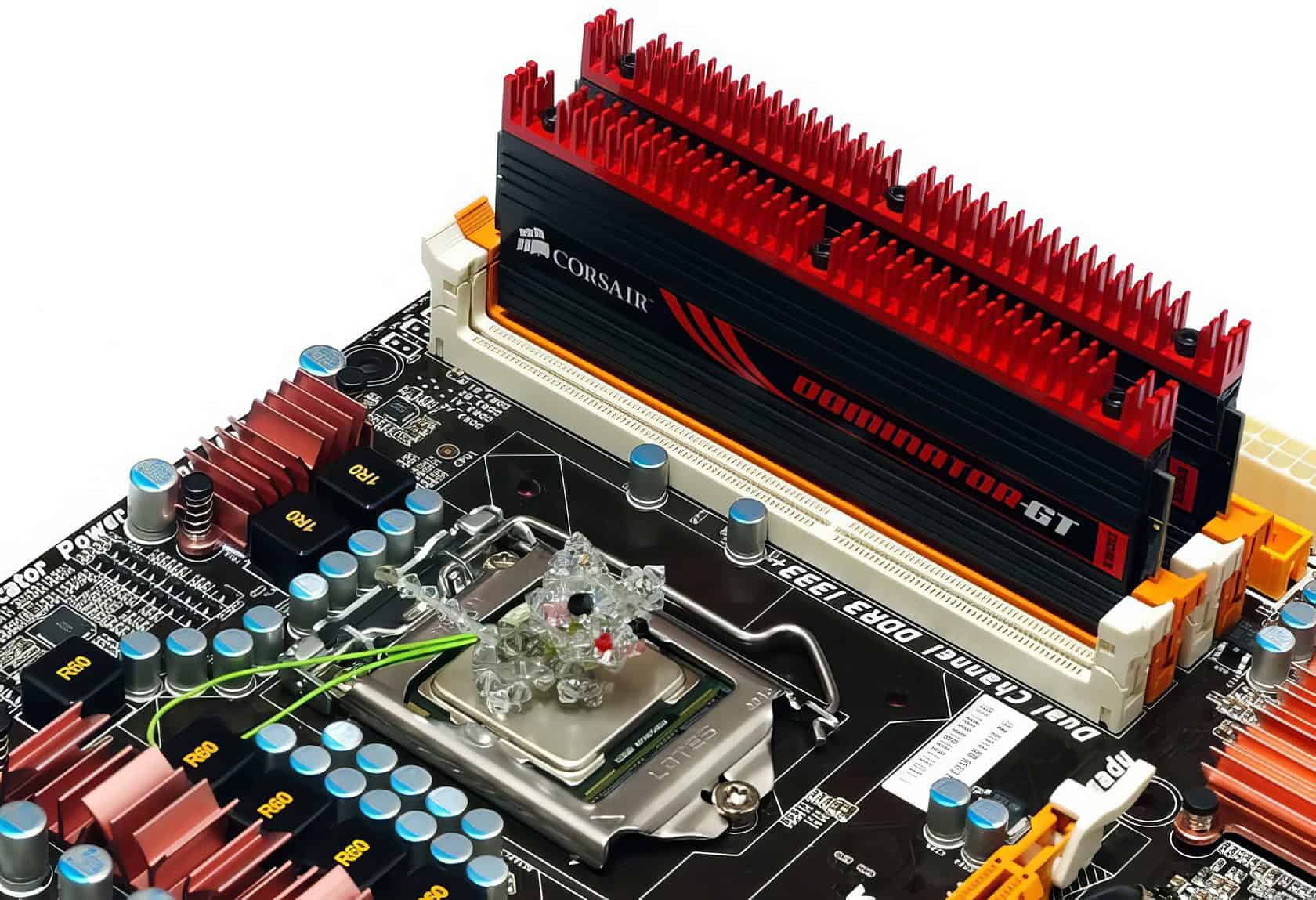
- Memory: 4GB of Kingston or CORSAIR DOMINATOR-GT DDR3 RAM, running at speeds up to 2000MHz when overclocked.
- Storage: A fast Kingston SSD was used for the operating system and applications to ensure storage wasn’t a bottleneck.
- Graphics: For discrete GPU tests, we used cards like the Zotac GTX 285 AMP! and the Radeon HD 5750 to see how Clarkdale performed with more graphics muscle.
- Power Supply: A reliable be quiet! E7 480W unit provided clean power. System power draw was impressively low, often around 34-39W at idle.
- Cooling: A Cooler Master Hyper 212 cooler kept the CPU temperatures in check during our overclocking and stress tests.
Which software tools and environment were used for testing?
With the hardware ready, we turned to a suite of software tools to measure every aspect of Clarkdale’s performance. All tests were conducted on a clean installation of Windows 7 Ultimate (64-bit) to ensure consistent and repeatable results.
The main tools in our arsenal included:
- BIOS/UEFI: The first stop for all overclocking, allowing direct control over BCLK, multipliers, and voltages.
- Intel Extreme Tuning Utility (XTU): Used for on-the-fly performance tweaking from within Windows.
- CPU-Z & GPU-Z: Essential utilities for verifying processor and graphics chip specifications and clock speeds.
- Prime95 & LinX: Our go-to stress tests for checking the stability of our overclocks.
- AIDA64 (formerly Everest): A comprehensive tool for deep system diagnostics, including memory latency benchmarks.
- HWMonitor: Our primary tool for keeping a close eye on CPU temperatures and system voltages.
- PCMark Vantage & 3DMark Vantage: Synthetic benchmark suites used to measure overall system performance and gaming potential.
Advantages of Intel’s 32nm Process Technology
Intel’s move to a 32nm manufacturing process was a huge leap forward. It allowed chips like the Core i3 and Core i5 to be faster, cooler, and more power-efficient, especially when paired with the new H55 and H57 chipsets.
How does the 32nm process enhance transistor performance?
Shrinking the manufacturing process to 32nm had a direct impact on performance. The smaller size allowed engineers to pack more transistors onto the chip, leading to faster data processing.
The use of second-generation high-k plus metal gate transistors was the real star of the show. This technology significantly reduced current leakage, a problem where electricity escapes from the transistors even when they’re switched off. By plugging these leaks, the chips ran much cooler and wasted less power. This efficiency is what allowed features like Turbo Boost to work so well, giving you extra performance without the risk of overheating your HTPC or gaming rig.
The 32nm process also enabled faster transistor switching speeds compared to older 45nm chips like the Core 2 Duo series. This helped accelerate everything from memory operations to graphics rendering on the integrated GPU.
What cost and size benefits does the 32nm die offer?
Moving to a 32nm die had huge benefits for both Intel and consumers. For Intel, shrinking the die meant they could produce more processors from a single silicon wafer, which dramatically lowered manufacturing costs.
These savings were passed on to buyers, with Clarkdale chips like the Core i3-530 launching at a very competitive $115. This put powerful, modern architecture within reach for budget-conscious builders.
The smaller size also meant these dual-core processors used less power, leading to lower electricity bills and cooler, quieter PCs. A smaller, more efficient chip was perfect for the growing market of microATX and HTPC builds. By integrating the CPU and integrated graphics into one compact package, you could build a powerful little machine without needing a bulky discrete graphics card, saving both space and money.
The Clarkdale Legacy: Was It Worth It?
Looking back, the Intel 32nm Clarkdale processors were a pivotal step in the evolution of the modern CPU. They weren’t the absolute fastest chips on the market, but they weren’t trying to be. Instead, they delivered a smart, balanced package that was perfect for the vast majority of computer users.
Clarkdale’s biggest win was its incredible efficiency. For the first time, you could build a small, quiet HTPC that could handle Blu-ray playback flawlessly and idle at under 30 watts, something that was a huge deal in 2010. It proved that you didn’t need a massive, power-hungry machine for a great everyday computing experience.
It was also a fantastic chip for tinkerers. The overclocking potential was massive for a mainstream processor, letting geeks squeeze out significant extra performance with just a decent air cooler and a bit of patience. While the integrated graphics couldn’t compete with dedicated gaming cards, it was more than enough for everyday tasks and even some light gaming on titles like Left 4 Dead.
Of course, it had its trade-offs, namely the higher memory latency due to its multi-chip design. But for its target audience, this was a minor issue. Clarkdale successfully brought the advanced Nehalem architecture (in its Westmere form) to an affordable price point, effectively ending the long reign of the Core 2 Duo and setting the stage for the highly integrated processors we use today. It was a true mainstream champion.
People Also Ask
What makes the Intel 32nm Clarkdale processors different from older chips like Core 2 Duo or Nehalem architecture?
Clarkdale introduced the first integrated graphics processor (IGP) packaged with the CPU, a major shift from the separate G45 chipset graphics. This was enabled by a die shrink to a 32nm process for the CPU cores, although the on-package graphics and memory controller remained on a 45nm die. This multi-chip design resulted in a smaller CPU die but also slightly increased memory latency compared to processors with a fully integrated memory controller.
How do H55, H57, and Q57 chipsets work with Clarkdale CPUs?
These chipsets were specifically designed with the Flexible Display Interface (FDI) needed to utilize Clarkdale’s integrated GPU for video output. The H55 was the base model for HTPC use, while the H57 added support for RAID via Intel Rapid Storage Technology and increased the number of USB ports from 12 to 14. The Q57 chipset was for business clients, including all H57 features plus remote management capabilities like Intel’s Active Management Technology (AMT).
Can you overclock the Core i5-661 using Turbo Boost?
You cannot directly overclock using Turbo Boost, as it’s an automatic feature that operates within Intel’s predefined thermal and power limits. However, the Core i5-661 was a capable overclocker by adjusting the base clock, with many users easily reaching 4.0 GHz on air cooling.
Is the integrated GPU good enough for HTPC use or light gaming?
The Intel Graphics Media Accelerator HD was excellent for HTPC tasks, smoothly decoding H.264 Blu-ray video with very low CPU usage. For gaming, it could handle older titles like World of Warcraft at low settings but was not powerful enough for demanding DirectX 10 games of its era.
How does power consumption compare between Clarkdale dual-core chips and something beefier like an Intel Core i7?
A Clarkdale dual-core like the Core i5-661 has a Thermal Design Power (TDP) of 87 watts, which is lower than a contemporary quad-core Lynnfield chip like the Core i7-870, which had a 95-watt TDP.
References
https://pcper.com/2009/09/intel-westmere-architecture-and-clarkdale-processor-preview/ (2009-09-27)
https://techgage.com/article/intels_32nm_clarkdale_-_nehalem_for_everyone/
https://www.tweaktown.com/news/13221/intel_s_32nm_cpus_show_good_power_usage/index.html (2009-09-28)
https://www.techreaction.net/post/3-step-overclocking-guide-for-clarkdale-processors
https://www.overclockers.com/i5-661-32nm-clarkdale-biostar-th55xe/
http://www.overclockers.com.au/article.php?id=838342&P=4
https://archive.org/stream/computer-power-user-magazine-v11i5/CPU_1105_djvu.txt
https://www.overclock.net/threads/exp-intel-s-32nm-clarkdale-processor-review-emerges.548993/ (2009-07-29)
https://techgage.com/article/intels_32nm_clarkdale_-_nehalem_for_everyone/9/
https://www.intc.com/news-events/press-releases/detail/1003/intel-demonstrates-industrys-first-32nm-chip-and (2007-09-18)
https://techgage.com/article/intels_32nm_clarkdale_-_nehalem_for_everyone/17/
